

 9470
9470
教程目的
适用对象
熟悉 Vivado 工程流程
对 FPGA 配置机制尚不深入,希望进入系统级设计阶段的学习者
Multiboot 功能概述
Multiboot Image:存放在 Flash 的其他地址,承载具体业务逻辑,可被升级或替换。
下图展示了 FPGA Multiboot 机制的整体配置与启动流程:FPGA 上电后默认从 Flash 0 地址加载 Golden Image,在满足触发条件后,通过 MultiBoot 机制尝试从 Upper Address 加载 MultiBoot Image。当配置成功时运行 MultiBoot Image;若配置失败,则触发 Fallback 机制,自动回退并重新加载 Golden Image,以保证系统仍可正常运行。
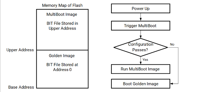
(Multiboot 运行流程示意图)
Multiboot 实现方式
Multiboot 实现方式
FPGA:AMD Artix UltraScale+(XCAU25P)
启动方式:SPI Flash(x4 模式)
该平台原生支持 MultiBoot 与 Fallback。
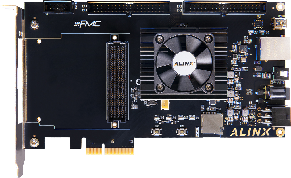
(ALINX基于Artix UltraScale+ FPGA开发板AXAU25)
//===========================================================================
// Module name: led_test.v
//===========================================================================
`timescale 1ns / 1ps
module multiboot_top
(
input sys_clk_p, // Difference system clock 200Mhz input on board
input sys_clk_n,
output reg led // LED,use for control the LED signal on board
);
//define the time counter
reg [31:0] timer;
wire [31:0] WBSTAR;
//===========================================================================
//Differentia system clock to single end clock
//===========================================================================
wire rst_n;
wire sys_clk_buf;
wire sys_clk;
wire switch;
wire switch_d0;
wire switch_d1;
IBUFGDS u_ibufg_sys_clk //????????????????
(
.I (sys_clk_p),
.IB (sys_clk_n),
.O (sys_clk_buf )
);
clk_wiz_0 syspll
(
// Clock out ports
.clk_out1(sys_clk), // output clk_out1
// Status and control signals
.locked(rst_n), // output locked
// Clock in ports
.clk_in1(sys_clk_buf));
vio_0 uu (
.clk(sys_clk), // input wire clk
.probe_out0(switch), // output wire [0 : 0] probe_out0
.probe_out1(WBSTAR) // output wire [31 : 0] probe_out1
);
//===========================================================================
//===========================================================================
always @(posedge sys_clk)
begin
if (~rst_n)
timer <= 32'd0; // when the reset signal valid,time counter clearing
else if (timer == 32'd99_999_999) //1 seconds count(200M-1=199999999) ?????200Mhz??????5ns??????0-199_999_999,??2*10^8??????
timer <= 32'd0; //count done,clearing the time counter
else
timer <= timer + 1'b1; //timer counter = timer counter + 1????????????????
end
//===========================================================================
// LED control
//===========================================================================
always @(posedge sys_clk)
begin
if (~rst_n)
led <= 0; //when the reset signal active
else if (timer == 32'd99_999_999) //time counter count to 1 sec,LED4 lighten
led <= ~led;
end
(* MARK_DEBUG="true" *)reg ce ;
(* MARK_DEBUG="true" *)reg write ;
(* MARK_DEBUG="true" *)reg [31:0] icap_in ;
(* MARK_DEBUG="true" *)wire [31:0] icap_in_wire ;
ICAPE3 #(
.DEVICE_ID(32'h04A64093), // Specifies the pre-programmed Device ID value to be used for simulation
// purposes.
.ICAP_AUTO_SWITCH("DISABLE"), // Enable switch ICAP using sync word.
.SIM_CFG_FILE_NAME("NONE") // Specifies the Raw Bitstream (RBT) file to be parsed by the simulation
// model.
)
ICAPE3_inst (
.AVAIL(), // 1-bit output: Availability status of ICAP.
.O(O), // 32-bit output: Configuration data output bus.
.PRDONE(), // 1-bit output: Indicates completion of Partial Reconfiguration.
.PRERROR(), // 1-bit output: Indicates error during Partial Reconfiguration.
.CLK(sys_clk), // 1-bit input: Clock input.
.CSIB(ce), // 1-bit input: Active-Low ICAP enable.
.I(icap_in_wire), // 32-bit input: Configuration data input bus.
.RDWRB(write) // 1-bit input: Read/Write Select input.
);
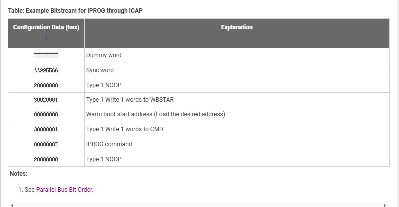
localparam [31:0] DUMMY_WORD = 32'hFFFFFFFF;
localparam [31:0] SYNC_WORD = 32'hAA995566;
localparam [31:0] TYPE1_NOOP = 32'h20000000;
localparam [31:0] TYPE1_WBSTAR = 32'h30020001;
localparam [31:0] TYPE1_CMD = 32'h30008001;
localparam [31:0] IPROG_CMD = 32'h0000000F;
// localparam [31:0] WBSTAR = 32'h04000000;
(* MARK_DEBUG="true" *)reg [3:0] state ;
assign icap_in_wire = {icap_in[3*8+0],icap_in[3*8+1],icap_in[3*8+2],icap_in[3*8+3],icap_in[3*8+4],icap_in[3*8+5],icap_in[3*8+6],icap_in[3*8+7],
icap_in[2*8+0],icap_in[2*8+1],icap_in[2*8+2],icap_in[2*8+3],icap_in[2*8+4],icap_in[2*8+5],icap_in[2*8+6],icap_in[2*8+7],
icap_in[1*8+0],icap_in[1*8+1],icap_in[1*8+2],icap_in[1*8+3],icap_in[1*8+4],icap_in[1*8+5],icap_in[1*8+6],icap_in[1*8+7],
icap_in[0*8+0],icap_in[0*8+1],icap_in[0*8+2],icap_in[0*8+3],icap_in[0*8+4],icap_in[0*8+5],icap_in[0*8+6],icap_in[0*8+7]};
always @(posedge sys_clk ) begin
if (~rst_n) begin
state <= 0 ;
ce <= 0 ;
write <= 0 ;
icap_in <= DUMMY_WORD ;
end
else begin
case (state)
0: begin
if (switch) begin
state <= 1 ;
icap_in <= DUMMY_WORD ; //Dummy word
write <= 0 ;
ce <= 0 ;
end
end
1: begin
state <= 2 ;
icap_in <= SYNC_WORD ; //sync word
end
2: begin
state <= 3 ;
icap_in <= TYPE1_NOOP ; //Type 1 NOOP
end
3: begin
state <= 4 ;
icap_in <= TYPE1_WBSTAR ; //Type 1 Write 1 words to WBSTAR
end
4: begin
state <= 5 ;
icap_in <= WBSTAR ; //Warm boot start address (Load the desired address)
end
5: begin
state <= 6 ;
icap_in <= TYPE1_CMD ; //Type 1 Write 1 words to CMD
end
6: begin
state <= 7 ;
icap_in <= IPROG_CMD ; //IPROG command
end
7: begin
state <= 8 ;
icap_in <= TYPE1_NOOP ; //Type 1 NOOP
end
8: begin
state <= 8 ;
write <= 1 ;
ce <= 1 ;
icap_in <= 0 ;
end
default: begin
state <= 0 ;
ce <= 1 ;
write <= 1 ;
icap_in <= DUMMY_WORD ;
end
endcase
end
end
endmodule
XDC 约束
############## clock define##################
create_clock -period 5.000 [get_ports sys_clk_p]
set_property PACKAGE_PIN T24 [get_ports sys_clk_p]
set_property PACKAGE_PIN U24 [get_ports sys_clk_n]
set_property IOSTANDARD DIFF_SSTL18_I [get_ports sys_clk_n]
##############LED define##################
set_property PACKAGE_PIN W21 [get_ports led]
set_property IOSTANDARD LVCMOS18 [get_ports led]
set_property CONFIG_MODE SPIx4 [current_design]
set_property BITSTREAM.CONFIG.CONFIGRATE 85.0 [current_design]
set_property BITSTREAM.CONFIG.SPI_32BIT_ADDR YES [current_design]
set_property BITSTREAM.CONFIG.SPI_BUSWIDTH 4 [current_design]
set_property BITSTREAM.CONFIG.SPI_FALL_EDGE YES [current_design]
set_property BITSTREAM.CONFIG.CONFIGFALLBACK ENABLE [current_design]
set_property BITSTREAM.GENERAL.COMPRESS TRUE [current_design]`timescale 1ns / 1ps
module multiboot(
//Differential system clock
input sys_clk_p,
input sys_clk_n,
input rst_n,
(* MARK_DEBUG="true" *) output reg [1:0] led
);
(* MARK_DEBUG="true" *)reg[31:0] timer_cnt;
wire sys_clk ;
IBUFDS IBUFDS_inst (
.O(sys_clk), // 1-bit output: Buffer output
.I(sys_clk_p), // 1-bit input: Diff_p buffer input (connect directly to top-level port)
.IB(sys_clk_n) // 1-bit input: Diff_n buffer input (connect directly to top-level port)
);
always@(posedge sys_clk)
begin
if (!rst_n)
begin
led <= 2'b0 ;
end
else if(timer_cnt <= 32'd100_000_000)
begin
led <= 2'b10;
end
else begin
led <= 2'b01;
end
end
always@(posedge sys_clk)begin
if(!rst_n)begin
timer_cnt <= 32'b0;
end
else if(timer_cnt >= 32'd199_999_999) //1 second counter, 200M-1=199_999_999
begin
timer_cnt <= 32'd0;
end
else begin
timer_cnt <= timer_cnt + 1;
end
end
endmodule
xdc约束
set_property PACKAGE_PIN T24 [get_ports sys_clk_p]
set_property PACKAGE_PIN N26 [get_ports rst_n]
set_property PACKAGE_PIN W21 [get_ports led]
set_property IOSTANDARD LVCMOS18 [get_ports {led[1]}]
set_property IOSTANDARD LVCMOS18 [get_ports {led[0]}]
set_property IOSTANDARD LVCMOS18 [get_ports rst_n]
set_property IOSTANDARD DIFF_SSTL18_I [get_ports sys_clk_p]
set_property PACKAGE_PIN AC16 [get_ports {led[0]}]
set_property PACKAGE_PIN W21 [get_ports {led[1]}]
create_clock -period 5.000 -name sys_clk_p -waveform {0.000 2.500} [get_ports sys_clk_p]
set_property BITSTREAM.CONFIG.CONFIGFALLBACK ENABLE [current_design]
set_property BITSTREAM.GENERAL.COMPRESS TRUE [current_design]
set_property BITSTREAM.CONFIG.SPI_BUSWIDTH 4 [current_design]
set_property BITSTREAM.CONFIG.SPI_32BIT_ADDR YES [current_design]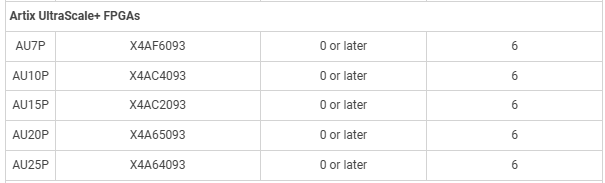
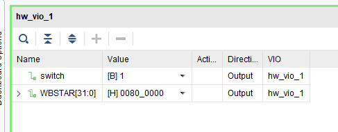
通过 VIO 设置
switch=1,WBSTAR=0x0080_0000(我们在 Flash 中存放的第二个 Multiboot Image 的初始地址),等待一段时间,LED 1、LED 2 交替闪烁,MultiBoot Image 切换成功。
参考文档
Vivado Design Suite 用户指南: 编程和调试 (UG908)
阅读全文